- 您现在的位置:买卖IC网 > Sheet目录2000 > IDTCV119EPVG8 (IDT, Integrated Device Technology Inc)IC CLK GEN DESKTOP PC 48-SSOP
COMMERCIALTEMPERATURERANGE
2
IDTCV119E
CLOCKGENERATORFORDESKTOPPCPLATFORMS
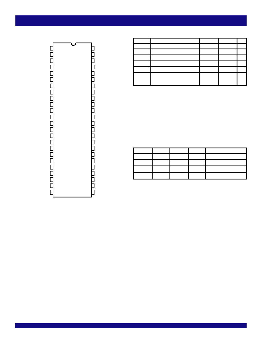
PIN CONFIGURATION
Symbol
Description
Min
Max
Unit
VDDA
3.3V Core Supply Voltage
4.6
V
VDDIN
3.3V Logic Input Supply Voltage GND - 0.5
4.6
V
TSTG
Storage Temperature
–65
+150
° C
TAMBIENT
Ambient Operating Temperature
0
+70
° C
TCASE
Case Temperature
+115
° C
ESD Prot
Input ESD Protection
2000
V
Human Body Model
ABSOLUTE MAXIMUM RATINGS(1)
NOTE:
1. Stresses greater than those listed under ABSOLUTE MAXIMUM RATINGS may cause
permanent damage to the device. This is a stress rating only and functional operation
of the device at these or any other conditions above those indicated in the operational
sections of this specification is not implied. Exposure to absolute maximum rating
conditions for extended periods may affect reliability.
SSOP
TOP VIEW
48
47
46
45
44
43
42
41
40
39
38
37
36
35
34
33
32
31
30
29
VDDA
VSS
IREF
VSS
CPUT1
CPUC1
VDD_CPU
CPUT0
CPUC0
VSS
SRCT
SRCC
VDD_SRC
*VTT_PWRGD#
*SDATA
*SCLK
RESET#
3V66_1
VSS
VDD_3V66
3V66_2
3V66_3/VCH
1
2
3
4
5
6
7
8
9
10
11
12
13
14
15
16
17
18
19
20
21
22
23
24
25
26
27
28
*FS1/REF0
*FS0/REF1
VDD_REF
X1
X2
VSS
PCIF0
PCIF1
PCIF2
VSS
PCI0
PCI1
PCI2
PCI3
VDD_PCI
VDD_PCI
PCI4
PCI5
*RESET#/PD#
**SEL24/24_48MHz#
48MHz0
VSS
VDD48
CPUT_ITP
CPUC_ITP
HW FREQUENCY SELECTION
FS1.0
CPU
AGP
PCI
N Resolution
00
100
66.66
33.3
0.223721591
01
200
66.66
33.3
0.447443181
10
133.33
66.66
33.3
0.298295454
11
166.67
66.66
33.3
0.397727272
* = ~ 130K
Ω internal pull-up.
** = ~ 130K
Ω internal pull-down.
发布紧急采购,3分钟左右您将得到回复。
相关PDF资料
IDTCV133PAG
IC FLEXPC CLK PROGR P4 56-TSSOP
IDTCV136PAG
IC FLEXPC CLK ATI RS400 56-TSSOP
IDTCV137PAG
IC FLEXPC CLK AMD K8 56-TSSOP
IDTCV142PAG
IC FLEXPC CLK PROGR P4 56-TSSOP
IDTCV146PVG
IC FLEXPC CLK PROGR P4 56-SSOP
IDTCV149PAG
IC FLEXPC CLK PROGR K8 56-TSSOP
IDTNW6005ASG
IC CALLER ID DECODER 20SOIC
IDTNW6006AS
IC CALLER ID DECODER 20-SOIC
相关代理商/技术参数
IDTCV122C
制造商:IDT 制造商全称:Integrated Device Technology 功能描述:PROGRAMMABLE FLEXPC? CLOCK FOR P4 PROCESSOR
IDTCV122CPVG
功能描述:IC FLEXPC CLK PROGR P4 56-SSOP RoHS:是 类别:集成电路 (IC) >> 时钟/计时 - 专用 系列:FlexPC™ 标准包装:28 系列:- 类型:时钟/频率发生器 PLL:是 主要目的:Intel CPU 服务器 输入:时钟 输出:LVCMOS 电路数:1 比率 - 输入:输出:3:22 差分 - 输入:输出:无/是 频率 - 最大:400MHz 电源电压:3.135 V ~ 3.465 V 工作温度:0°C ~ 85°C 安装类型:表面贴装 封装/外壳:64-TFSOP (0.240",6.10mm 宽) 供应商设备封装:64-TSSOP 包装:管件
IDTCV122CPVG8
功能描述:IC FLEXPC CLK PROGR P4 56-SSOP RoHS:是 类别:集成电路 (IC) >> 时钟/计时 - 专用 系列:FlexPC™ 标准包装:28 系列:- 类型:时钟/频率发生器 PLL:是 主要目的:Intel CPU 服务器 输入:时钟 输出:LVCMOS 电路数:1 比率 - 输入:输出:3:22 差分 - 输入:输出:无/是 频率 - 最大:400MHz 电源电压:3.135 V ~ 3.465 V 工作温度:0°C ~ 85°C 安装类型:表面贴装 封装/外壳:64-TFSOP (0.240",6.10mm 宽) 供应商设备封装:64-TSSOP 包装:管件
IDTCV123
制造商:IDT 制造商全称:Integrated Device Technology 功能描述:PROGRAMMABLE FLEXPC CLOCK FOR P4 PROCESSOR
IDTCV123PV
功能描述:IC FLEXPC CLK PROGR P4 56-SSOP RoHS:否 类别:集成电路 (IC) >> 时钟/计时 - 专用 系列:FlexPC™ 标准包装:1,500 系列:- 类型:时钟缓冲器/驱动器 PLL:是 主要目的:- 输入:- 输出:- 电路数:- 比率 - 输入:输出:- 差分 - 输入:输出:- 频率 - 最大:- 电源电压:3.3V 工作温度:0°C ~ 70°C 安装类型:表面贴装 封装/外壳:28-SSOP(0.209",5.30mm 宽) 供应商设备封装:28-SSOP 包装:带卷 (TR) 其它名称:93786AFT
IDTCV123PV8
功能描述:IC FLEXPC CLK PROGR P4 56-SSOP RoHS:否 类别:集成电路 (IC) >> 时钟/计时 - 专用 系列:FlexPC™ 标准包装:1,500 系列:- 类型:时钟缓冲器/驱动器 PLL:是 主要目的:- 输入:- 输出:- 电路数:- 比率 - 输入:输出:- 差分 - 输入:输出:- 频率 - 最大:- 电源电压:3.3V 工作温度:0°C ~ 70°C 安装类型:表面贴装 封装/外壳:28-SSOP(0.209",5.30mm 宽) 供应商设备封装:28-SSOP 包装:带卷 (TR) 其它名称:93786AFT
IDTCV123PVG
功能描述:IC FLEXPC CLK PROGR P4 56-SSOP RoHS:是 类别:集成电路 (IC) >> 时钟/计时 - 专用 系列:FlexPC™ 标准包装:1,500 系列:- 类型:时钟缓冲器/驱动器 PLL:是 主要目的:- 输入:- 输出:- 电路数:- 比率 - 输入:输出:- 差分 - 输入:输出:- 频率 - 最大:- 电源电压:3.3V 工作温度:0°C ~ 70°C 安装类型:表面贴装 封装/外壳:28-SSOP(0.209",5.30mm 宽) 供应商设备封装:28-SSOP 包装:带卷 (TR) 其它名称:93786AFT
IDTCV123PVG8
功能描述:IC FLEXPC CLK PROGR P4 56-SSOP RoHS:是 类别:集成电路 (IC) >> 时钟/计时 - 专用 系列:FlexPC™ 标准包装:28 系列:- 类型:时钟/频率发生器 PLL:是 主要目的:Intel CPU 服务器 输入:时钟 输出:LVCMOS 电路数:1 比率 - 输入:输出:3:22 差分 - 输入:输出:无/是 频率 - 最大:400MHz 电源电压:3.135 V ~ 3.465 V 工作温度:0°C ~ 85°C 安装类型:表面贴装 封装/外壳:64-TFSOP (0.240",6.10mm 宽) 供应商设备封装:64-TSSOP 包装:管件